How is a weight transmitter made?
All the production phases of a LAUMAS weight transmitter.
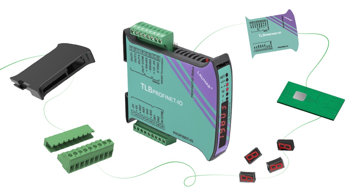
From the design of the weight transmitters and indicators to the final testing and marketing of the finished products: at LAUMAS we take care over all the phases of production of our electronic weighing instrumentation, ensuring high standards of quality at every step.
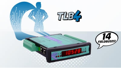
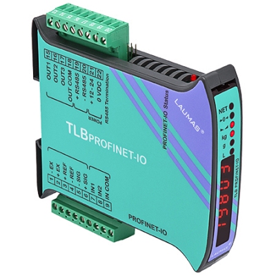
Let’s take a close look at the birth of a TLB PROFINET IO weight transmitter.
Table of contents
1. The printed circuit board
2. Acceptance and storage of electronic components
3. Machine setting
4. Production start up
5. The "golden board"
1. The printed circuit board
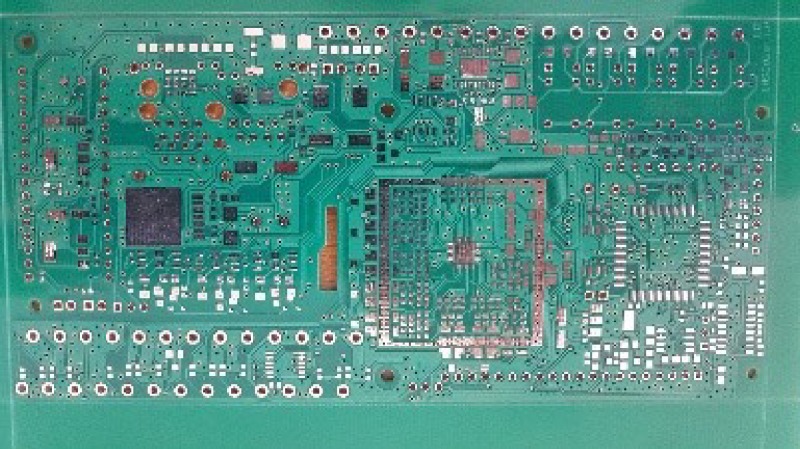
Weight transmitter production starts exactly here: with the Printed Circuit Board (PCB), a bare board manufactured specifically for LAUMAS based on the instructions of the Research & Development d
The Surface Mounting Device (SMD) electronic components, i.e. the components mounted on the surface of the board, which are to form the beating heart of our weight transmitter, will be positioned and soldered on the exposed parts of each printed circuit board (pads).
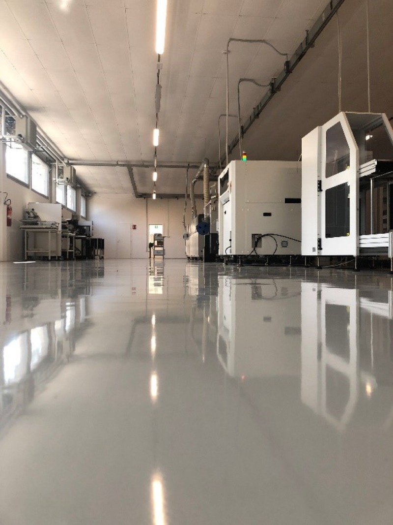
The antistatic flooring of the LAUMAS weighing electronics production department.
The electronic components are extremely sensitive to electrostatic charges.
To avoid potential damage the floor of the production department is antistatic: it is completely covered with a special resin, made conductive by the presence of carbon fibers, in which is sunk a copper grid connected to the grounding of the electrical system.
All workers wear antistatic footwear so as to be at the same potential as the grounding of the system.
2. Acceptance and storage of electronic components
We pay special attention to the traceability of the electronic components to be soldered onto the printed circuit.
At the stage of acceptance, we label each component with a unique QR code identifying the entire supply chain: manufacturer data records code, production batch and transport document references.
In selecting the components we source, we are sensitive to compliance with the Conflict Mineral Policy Statement.
In response to violence and to violations of human rights in the mining of certain minerals in the eastern area of the Democratic Republic of the Congo, we are committed to promoting the traceability of these minerals and the transparency of the supply chain ensuring that only conflict free materials and components are used.
All the components are then stored in a warehouse that controls both temperature (below 22°C) and humidity (below 10%), to avoid any alterations to the components.
Each production job order has a code to which all the quantities to be produced and the various planned working phases are linked.
The automatic warehouse reports inventories and verifies that it contains all the components needed to proceed with the production of the job order.
Once the job order has been received and the components have been verified, an automatic arm selects them, takes them from the drawers and places them on a shelf.
The operator picks up the components and places them on a carriage to transfer them to the next working phases.
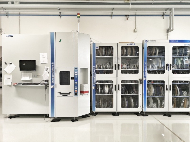
Automated warehouses with temperature and humidity controls of the components located inside.
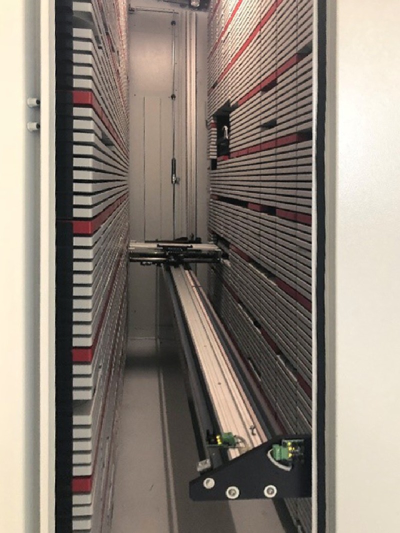
The mechanical arm, in the automated warehouse, extracts the drawers containing the electronic components.
3. Machine setting
After preparing all the components for making the weight transmitter, the machines are set.
Screen printed machine
The operator places the following items inside the machine: the screen printing foil, a steel plate equipped with precise holes matching the predefined pads of the printed circuit board on which the components are to be placed and soldered.
The foil acts as a stencil: through its holes the machine precisely dispenses the solder paste needed for soldering on the pads of the PCB.
Pick and Place
The operator selects the feeders by choosing their size according to the type of component to be installed.
He then inserts the coils with the components in the corresponding feeders and positions them following a precise numbering order indicated by the machine.
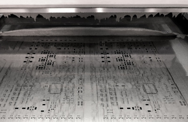
The screen printing foil, which serves as a stencil for precisely dispensing the solder paste.
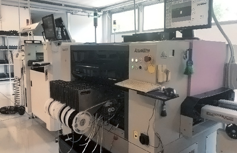
The Pick and Place machine, with the reels of components inserted in the feeders.
It is important to perform annual maintenance on the machines to ensure their correct calibration and consequently their precision.
In fact, having to assemble microcomponents that may measure as little as a few tenths of a millimeter, even the slightest shift would pose a problem.
4. Production start-up
Once the preparatory phases have been completed, work begins on the electronic board.
The screen printing process
The screen printing machine deposits the solder paste at the holes in the stencil i.e., on the points of the board where the Pick and Place” machine will place the components to be soldered.
It is a high-precision device: before proceeding to dispense paste, software dedicated to machine management verifies that the screen printing foil is perfectly centered on the board.
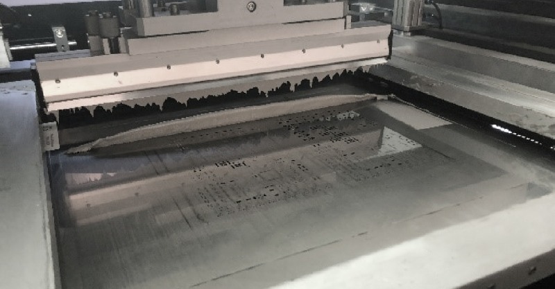
Screen printing machine for dispensing solder paste on the PCB.
The Pick and Place machine
Very fast and extremely precise, the Pick and Place proceeds to assemble the SMD components on the electronic board.
Using a vacuum system, the machine picks up the components.
Using a video camera it processes an image of the process that evaluates the suitability of each component based on parameters such as dimensions and rotation.
If the component is suitable, it is deposited on the board; if not, it is discarded in the so-called “dump box”.
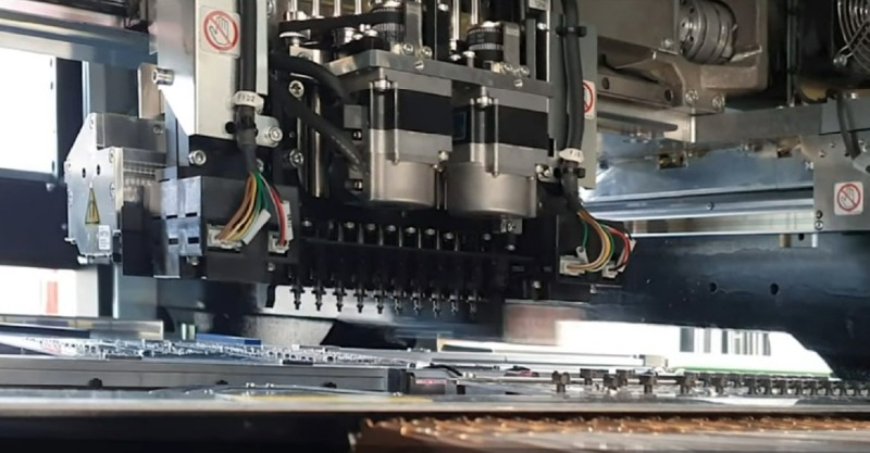
Detail of the Pick and Place machine in operation.
Suitable components are simply placed on the PADS of the printed circuit board, on which the screen printing machine has already dispensed the solder.
The exact point on the board where the component is deposited is the result of the design developed by our Research and Development department, transferred to a file and imported into the machine.
The Pick and Place is actually a line consisting of 2 machines: one assembles the smaller components, called chips (resistors, capacitors, diodes, transistors), while the other handles the larger components (integrated circuits, microprocessors, and connectors).
This avoids interrupting production to change tools, which differ depending on the dimensions of the components: the machine is always running, the work is optimized and speeded up, and high standards in terms of performance are guaranteed.
5. The "golden board"
The first assembled electronic board leaves the machines and passes into the hands of the operator who analyzes it and verifies that everything matches the project shown on the bill of materials (BOM): the official document specifying the type and value of each component at each location on the board.
If the first board passes the inspection perfectly, it becomes the “golden board”, i.e. the verified and validated reference measurement standard board, which meets all the expected design standards.
The “golden board” will serve as a reference point in the production process to ensure that boards produced subsequently are consistent with it, ensuring uniformity in the quality and overall performance of the final product.
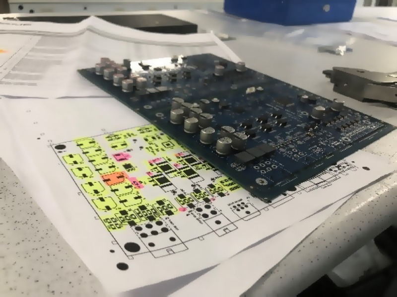
The electronic board validated as the 'golden board' with the bill of materials.
When we talk about "value" in a list of components for assembling an electronic board, we are referring to the following specifications:
-
Electrical value: refers to electrical parameters such as resistance, capacitance, inductance.
-
Tolerances: indicate how much the actual value may deviate from the nominal value.
-
Physical characteristics: dimensions, weight, and shape, which may affect the assembly and the design of the board.
6. Reflow soldering in an oven
After solder paste is applied and after assembly, the electronic board goes into the reflow oven for soldering the components.
The reflow oven is an advanced system designed to provide a highly controlled heating and cooling process, ideal for melting and remelting the metal alloys contained in the solder cream.
The oven consists of 8+8 heating zones (present at both the top and bottom) and 2 cooling zones.
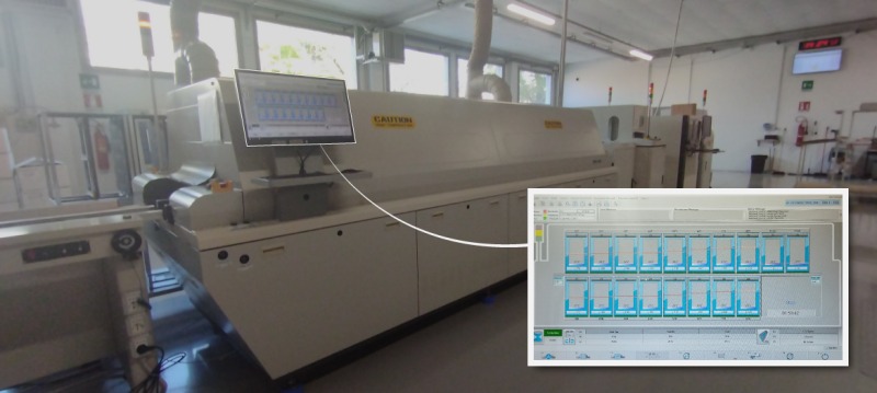
Reflow oven with 8+8 heating zones + 2 cooling zones.
The solder paste is remelted in the oven where it passes from the liquid state to a solid following a precise thermal profile, indicated by the solder cream manufacturers.
In fact, each solder paste has its own specific characteristics and, in order to obtain a correct soldering profile, it must remain in the different zones of the oven at precise temperatures and for defined times.
To verify that the temperature profile is always correct, it is checked periodically through calibrated temperature profilers certified by the designate
The profiler uses sensors and monitoring systems to analyze and control the temperature and flow of air inside the oven.
Its main purpose is to ensure that the metal contained in the solder creams is heated evenly and that during the reflow process the desired thermal profile characteristics are maintained.
Precise temperature control is essential to prevent defects in the final product.
Also the solder paste used is always certified, guaranteeing compliance with all the soldering parameters that ensure its quality, tightness and reliability over time.
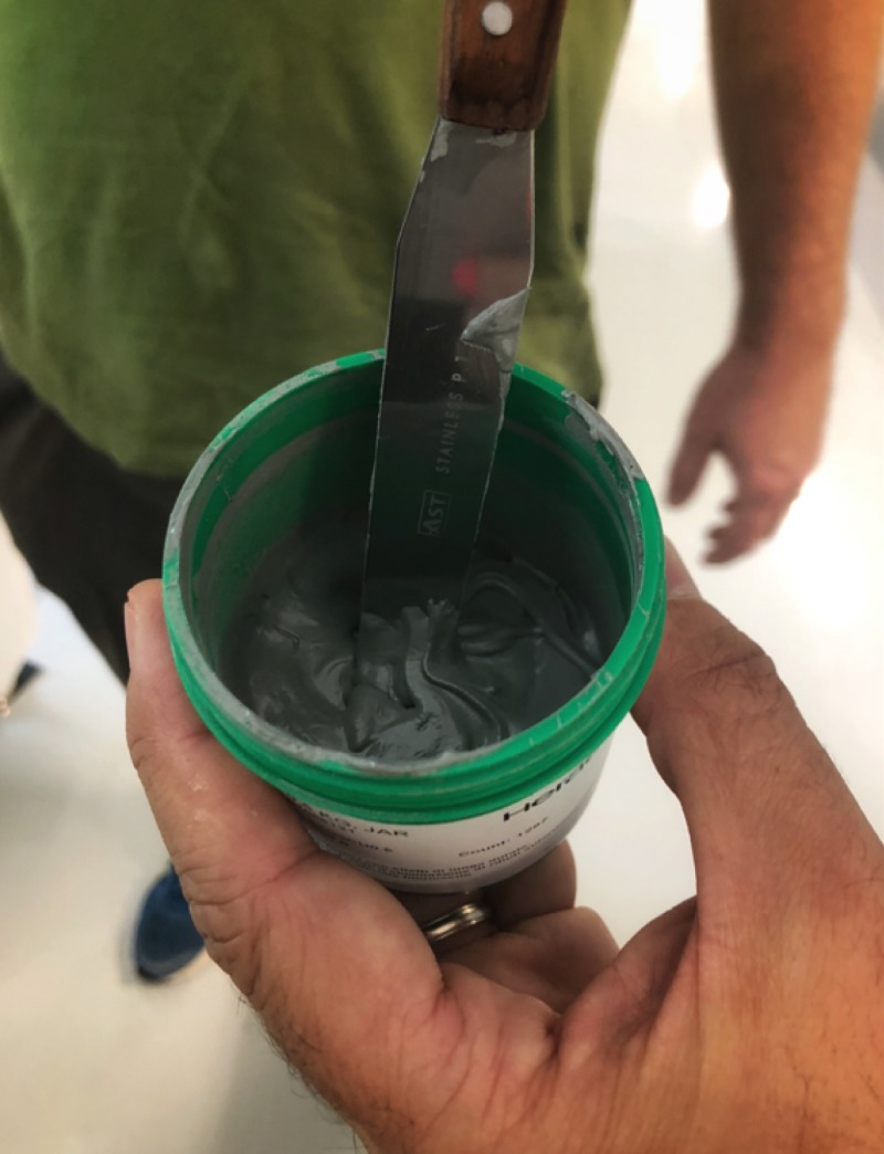
The solder paste we use is a lead-free formulation that complies with various standards and certifications, which include:
-
ROHS: a directive restricting the use of hazardous substances in electronic devices.
-
REACH: a European regulation on the registration, evaluation, authorization and restriction of chemicals.
-
ISO 9001: certification that guarantees a quality management system in production.
-
IPC: a standard specific to the electronics industry covering soldering quality and product performance.
7. 3D optical inspection
After soldering the components to the printed circuit board, automatic optical inspection (3D AOI) is performed on the electronic boards.
The operator inserts the boards into an ultra-high technology machine that analyzes all the components, reconstructing a detailed three-dimensional image of them.
This allows him to thoroughly check both each single component and its soldering and to verify several factors:
- the presence or absence of components on the board and their polarity;
- The soldering joint and its compliance with the parameters required by IPC quality standards
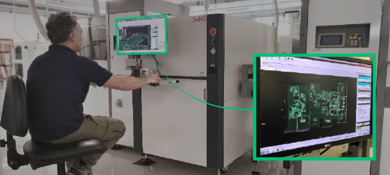
Machine for 3D optical inspection of the electronic boards.
In conjunction with AOI machines, it is also possible to use those with X-rays.
X-ray analysis of the electronic board is used to see the correctness of the internal interconnections of components. It is useful for identifying defects, verifying the integrity of the soldering and analyzing the circuit layout.
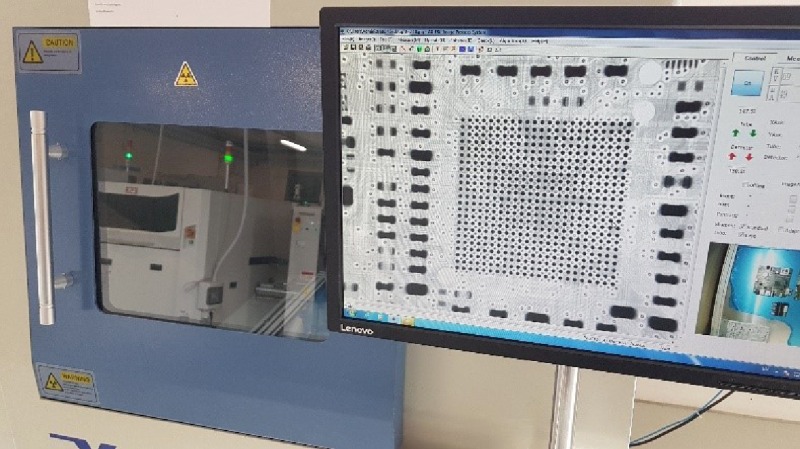
Machine for X-ray analysis of the electronic board.
8. Manual assembly and selective soldering machine
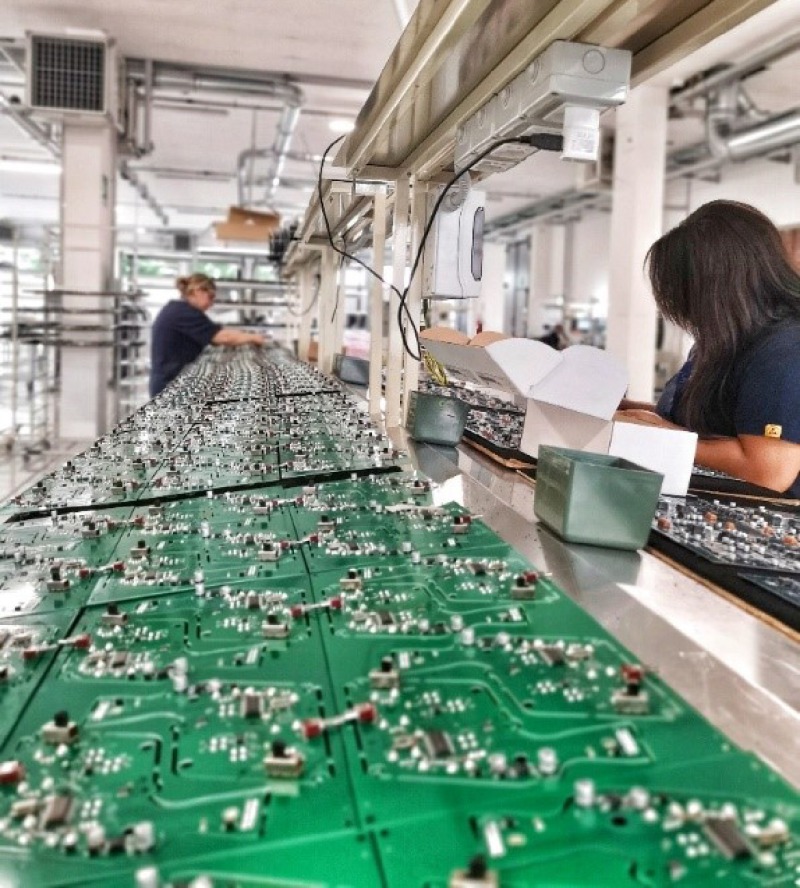
Semi-finished electronic boards validated as perfect by 3D optical inspection are ready for manual assembly.
In fact, not all the components of a board can be assembled by means of a machine: some must be positioned by hand by skilled operators, with the aid of specific equipment and following the assembly diagram of the technical documentation created by the R&D department.
The components that are manually assembled are the so-called THC (Through Hole Components), such as keys, displays, electrolytic capacitors, inductors, power supply leads, Ethernet connectors, LEDs, terminals.
The components positioned by hand must then also be soldered. Depending on the type of electronic board, 2 different machines are used:
▷ Solder wave soldering machine: this is the traditional soldering machine, which solders all the components at once.
It is used for simpler electronic boards, which have components only on the top.
▷ Selective soldering machine: this is the soldering machine that uses a nozzle to spot-solder the single components.
It is used for the most complex electronic boards to handle, that is, those that have components on both the top and bottom (double-sided boards).
Although the TLB Profinet weight transmitter board is not the double-sided type, we still use a selective soldering machine because it creates less thermal stresses on the board resulting in higher performance.
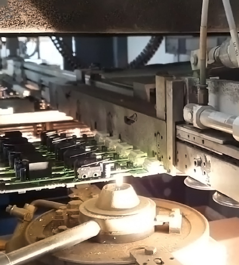
Selective soldering of a double-sided board.
9. Testing, board completion and firmware programming
Upon completing production of the electronic board, the last checks after soldering are carried out and then the next steps:
- labeling and mounting the display;
- programming, by which the firmware is installed in the weight transmitter microprocessor;
- testing the fieldbus.
Afterwards, the electronic boards are mechanically closed and placed in the appropriate containers.
This step takes place before final testing to ensure that after passing the test the product is no longer handled, thus avoiding the risk of any damage.
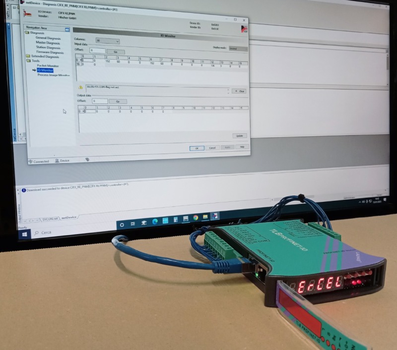
TLB Profinet IO weight transmitter fieldbus final test phase.
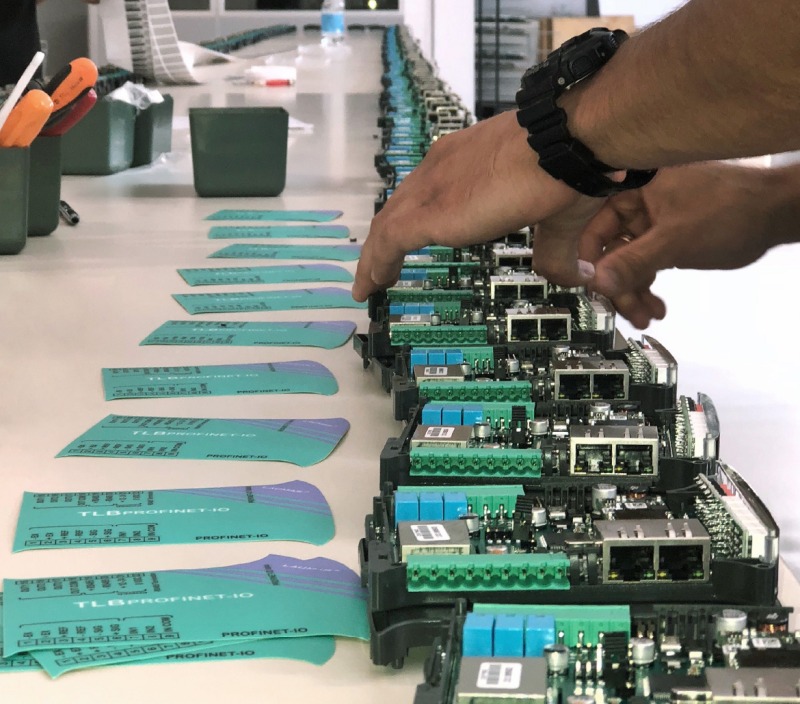
Electromechanical assembly of an electronic board: expert technicians precisely join the electronic boards with their plastic containers.
10. Final testing
Final testing of the weight transmitters is the last step in production.
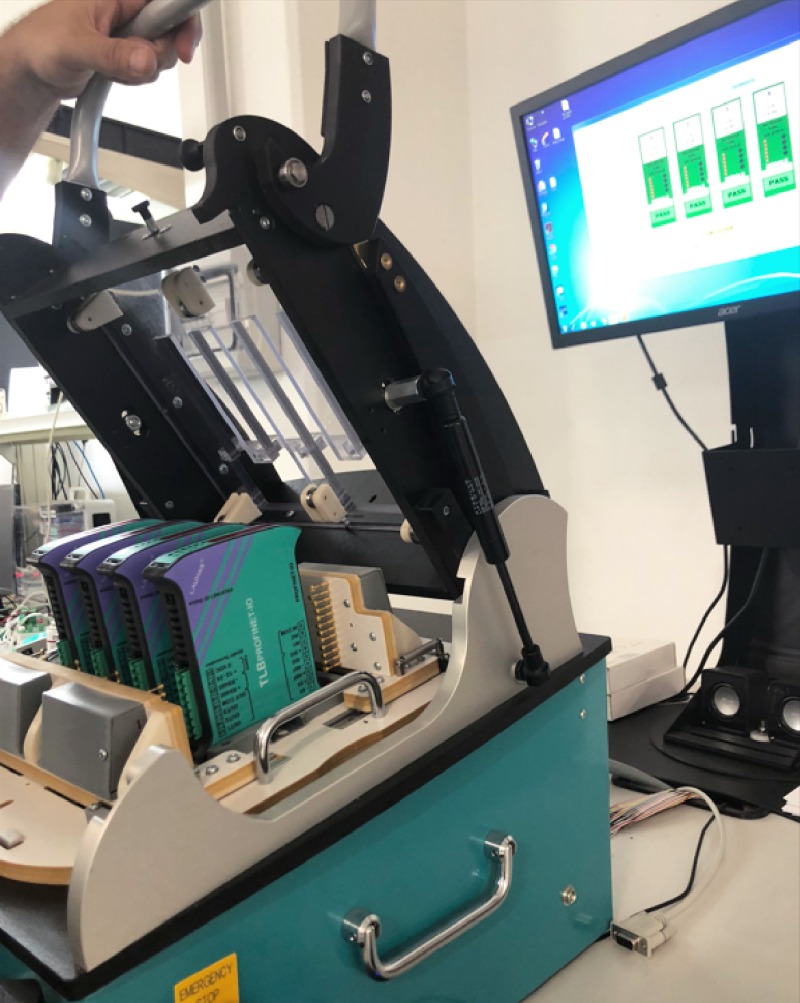
The testing station used to check the weight transmitters work properly.
The operator places the product inside the testing station, where a system running on linear guides connects to the instrument terminal blocks via gold-plated contacts.
At this point, in the testing software, the operator indicates the model of the instrument board to be tested (in this case TLB PROFINET IO), to which are associated a set of parameters to be verified.
The test begins with the simplest controls, such as power supplies, inputs, serial and analog outputs and the power consumption of the board.
The operation of the instrument is then simulated with a load cell simulator that verifies the theoretical calibration, the linearity and everything else that the research and development department considers essential to ensure maximum reliability and repeatability of the weight transmitter.
At the same time, the operator checks the LEDs, displays and keys.
After also passing final testing, the TLB PROFINET IO weight transmitter is ready to be marketed.
منتجات ذات صلة
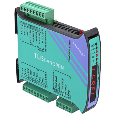
TLB CANOPEN
Weight transmitters
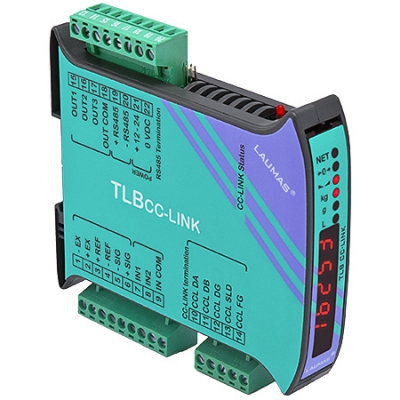
TLB CC-LINK
Weight transmitters
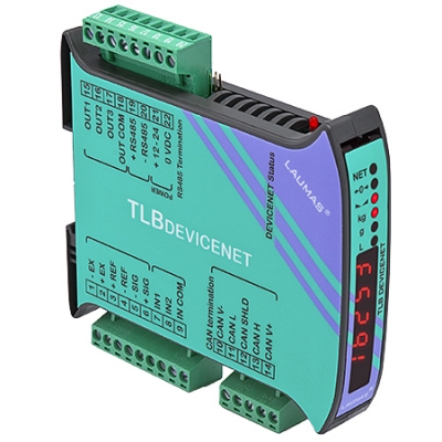
TLB DEVICENET
Weight transmitters
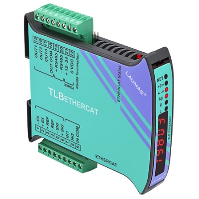
TLB ETHERCAT
Weight transmitters
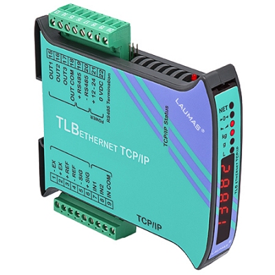
TLB ETHERNET TCP/IP
Weight transmitters
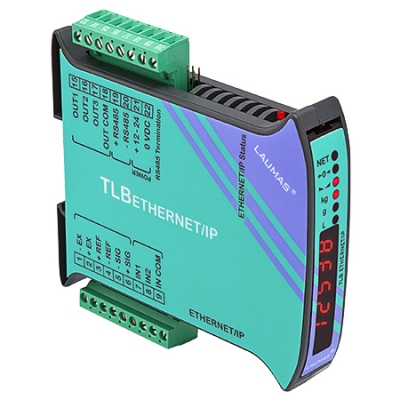
TLB ETHERNET/IP
Weight transmitters
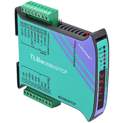
TLB MODBUS/TCP
Weight transmitters
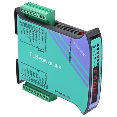
TLB POWERLINK
Weight transmitters
TLB PROFINET IO
Weight transmitters
TLB SERCOS III
Weight transmitters

